In fact, semiconductor manufacturing is one of the industrial activities that require strictest precision, discipline and infrastructure standards.
How is a semiconductor chip made?
A semiconductor chip is not a simple material block but an ultra-complex structure made up of hundreds of ultra-thin layers, each having a specific function and distinct physical-chemical properties. To create these layers, a chip plant must master multiple core technologies. Every layer goes through seven mandatory steps, namely cleaning, deposition, photolithography, etching, ion implantation, thermal annealing, and planarization. No step is optional, no shortcut is allowed. The process is closed-loop, sequential, and repeated hundreds of times until the chip is complete.
    |
 |
|
Chip manufacturing leaves zero room for error. |
The process starts with silicon wafer with near-absolute purity: only one impurity atom per one billion silicon atoms is tolerated. Before entering the production line, wafers must be perfectly clean as a single microscopic dust particle can ruin the entire circuit.
In the deposition stage, metal or dielectric layers are formed on the wafer using chemical reactions or physical vapor techniques. Each layer is only atoms thick, requiring extreme precision in temperature, pressure, and timing. Even the smallest deviation can destroy the layer’s designed properties.
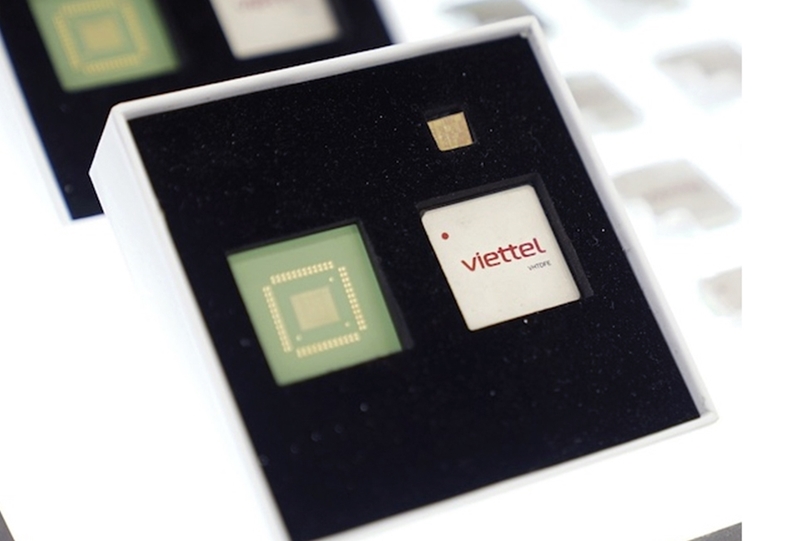
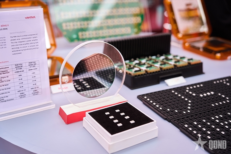
Photolithography is considered the heart of chip manufacturing, where billions of transistors are patterned onto an area no larger than a fingernail. This stage requires the most complex and expensive equipment in the factory. A photolithography machine costs around USD 400 million.
The wafer is coated with photoresist materials and projected to ultraviolet light through a mask to define precise circuit patterns.
The next step is etching, where plasma ions and chemical reactions carve circuit patterns into the thin films.
Ion implantation and thermal annealing fine-tune the electrical properties, while planarization ensures surface flatness for the next layer. Throughout the process, measurement and inspection play a decisive role in ensuring yield and performance.
|
|
 |
|
It takes 1,000 steps to turn a silicon wafer into a semiconductor chip. |
In total, a wafer undergoes around 1,000 processing steps.
Chip plant: industrial complexes with highest standards
A wafer typically circulates inside the factory for about three months, traveling tens of kilometers through hundreds of machines.
In large factories, the total daily wafer transport distance can reach 240,000 km, equivalent to six trips around the Earth. Thus optimizing wafer movement alone is a massive operational challenge.
A chip fab houses cleanrooms spanning several hectares, hundreds of machines worth millions to hundreds of millions of dollars, operating non-stop. It must manage over 300 types of materials, gases, and chemicals, all under strict control.
Infrastructure requirements are equally extreme: Power consumption equals that of around 50,000 households, with ultra-high stability since seconds of voltage drop can cause millions of dollars in losses; water must be ultra-pure, with organic carbon below one part per billion, about 2,000 times cleaner than drinking water; cleanrooms must meet Class 1 standards: No more than 35 dust particles per cubic meter, 10,000 times cleaner than an operating room; vibrations are limited to 12.5 micrometers per second, levels imperceptible to humans but critical for chip manufacturing.
These near-absolute standards explain why only a handful of countries can successfully build and operate semiconductor fabs.
|
|
 |
|
Viettel’s semiconductor factory is scheduled to be operational from 2027. |
In this context, Viettel role in leading and operating Vietnam’s high-tech semiconductor fab carries high significance.
At the groundbreaking ceremony, Lieutenant General Tao Duc Thang, Chairman and General Director of Viettel Group, stated that Vietnam’s first chips carrying Vietnamese intelligence would be created here, forming the foundation of a self-reliant, modern, globally integrated semiconductor industry. Viettel is committed to a military-style discipline: progress as law, quality as standard, safety as principle, contributing concrete results to Vietnam’s semiconductor strategy.
Translated by Mai Huong